Fusion Chip పితామహుడు శ్రీ గుదె దశరథ రామాంజనేయులు
Fusion Chip పితామహుడు శ్రీ గుదె దశరథ రామాంజనేయులు
https://www.megamindsindia.in/2025/09/dasaradha-gude-amd-fusion-chip.html
2030 కల్లా ప్రపంచ SemiConductor Manufacturing Hub గా భారత్
https://www.megamindsindia.in/2025/09/india-global-semiconductor-manufacturing-hub.html
సెమీకండక్టర్ విప్లవం – ప్రపంచాన్ని మార్చిన తెలుగు తేజం దశరథ రామ్ గుదె
https://www.megamindsindia.in/2025/09/semiconductor-revolution-telugu-visionary-dasaradha-ram-gude.html
Innovation - NASSCOM SME Inspire Awards 2022-23
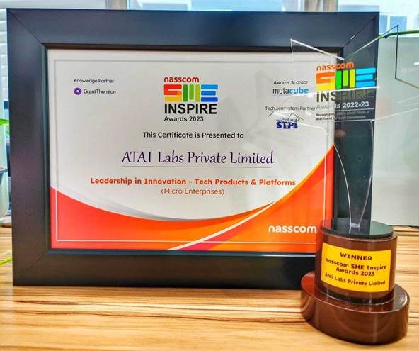
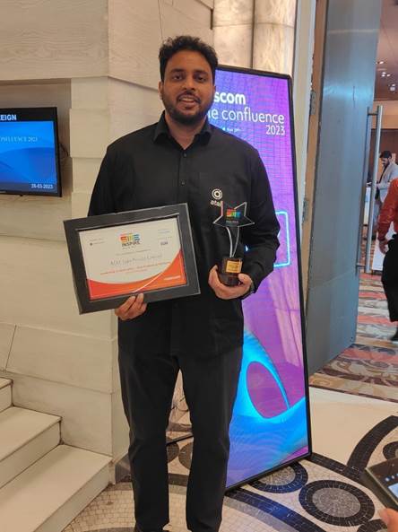
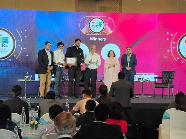
Winner of NASSCOM - Manufacturing Innovation Challenge (MIC 3.0) 2021
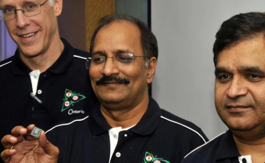
It is heartening to note that Mr. Gangadhar Gude, Founder and CEO, ATAI Labs is an alumni of VEDA IIT.
VLSI Exposure Training
పత్రిక ప్రకటన 31.07.2021
VLSI పాఠ్యాంశాలకు ఆరు రోజుల్లో….అనూహ్య స్పందన • ఇంజనీరింగ్ విద్యార్థుల ఆసక్తి – ప్రతి రోజూ 60వేల వ్యూస్ • విదేశాల్లోని విద్యార్థులకూ ఉపయోగపడే పాఠ్యాంశాలు • టి-సాట్ యాప్ ప్లే లిస్ట్, యూట్యూబ్ లో అందుబాటులో కంటెంట్ • భవిష్యత్ లో మరిన్ని ప్రసారాలకు సిద్దమౌతున్న ప్రభుత్వం (టి.సాట్ – సాఫ్ట్ నెట్) తెలంగాణ ప్రభుత్వ టి-సాట్ నెట్వర్క్ ఛానళ్ల ద్వార ప్రసారం చేస్తున్న VLSI ఎలక్ట్రానిక్స్ సెమీ కండక్టర్స్ పాఠ్యాంశ ప్రసారాలకు మంచి ఆదరణ వస్తోంది. ప్రసారాలు ప్రారంభించిన ఆరు రోజుల్లోనే అనూహ్య స్పందన లభించింది. VLSI ప్రసారాలకు వస్తున్న స్పందనపై టి-సాట్ సీఈవో ఆర్.శైలేష్ రెడ్డి శనివారం పత్రిక ప్రకటన విడుదల చేశారు. ఈ నెల 26వే తేదీన VLSI పై ప్రారంభించిన పాఠ్యాంశ ప్రసారాలకు రోజుకు 60 వేల మంది చొప్పున విద్యార్థులు ఫాలో అవుతున్నారని తెలిపారు. టి-సాట్ యాప్, యూట్యూబ్ స్టాటిస్టిక్స్, టీవి ఛానళ్లు విద్య, నిపుణతో పాటు ఫొటానిక్స్ వాలీ నిర్వహించిన సర్వే ద్వార VLSI కార్యక్రమాన్ని ఇంజనీరింగ్ విద్యార్థులు భారీ సంఖ్యలో అనుసరిస్తున్న విషయం స్పష్టమైందని శైలేష్ రెడ్డి తెలిపారు. గంట డ్యూరేషన్ గల రెండు వీడియోలను ఉదయం 8.15 నుండి 10.30 గంటల వరకు ప్రతి రోజూ ప్రసారం చేస్తుండగా గత ఆరు రోజుల్లో 12 పాఠ్యాంశాలకు 9,985 వ్యూస్ లభించాయని, సాయంత్రం ఏడు నుండి తొమ్మిది గంటల వరకు పున: ప్రసారమైన పాఠ్యాంశాలను సుమారు 26,535 ఇంజనీరింగ్ విద్యార్థులు అనుసరించారని సీఈవో స్పష్టం చేశారు. ఫొటానిక్స్ వ్యాలీ సంస్థ వద్ద నమోదైన విద్యార్థుల లెక్కల ప్రకారం సుమారు 3,000 మంది ఫాలో అవుతుండగా డీటీహెచ్, కేబుల్ నెట్వర్క్, ఫేస్ బుక్ ద్వారా వేలాది మంది విద్యార్థులు వి.ఎల్.ఎస్.ఐ పాఠ్యాంశాల ద్వార ప్రత్యేక అవగాహన పొందుతున్నారన్నారు. ప్రస్తుతం ఉదయం, సాయంత్రం వేలల్లో ప్రసారమయ్యే VLSI పాఠ్యాంశాల URL links వెబ్సైట్, టి-సాట్ యాప్ ప్లే లిస్టులలో అందుబాటులో ఉంటాయని సీఈవో శైలేష్ రెడ్డి తెలిపారు.
విదేశాల్లోని విద్యార్థులూ చూడవచ్చు
VLSI పాఠ్యాంశాలకు ప్రపంచ ప్రాధాన్యత ఉన్నందున విదేశాల్లో ఉన్న భారత విద్యార్థులూ చూడవచ్చని శైలేష్ రెడ్డి స్పష్టం చేశారు. అడ్వకేట్ జనరల్ రాజగొపాల్ VLSI పాఠ్యాంశాల ప్రత్యక్ష్య ప్రసారం సందర్భంగా టి-సాట్ స్టూడియోకు ఫోన్ ద్వార మాట్లాడి తన అనుమానాలను నివృత్తి చేసుకున్నారు. ‘మా పిల్లలు విదేశాల్లో నివసిస్తున్నారు. టి-సాట్ ద్వార ప్రసారమయ్యే పాఠ్యాంశాలు అందరికీ ఉపయోగపడేవిగా ఉన్నాయి. తెలంగాణ ప్రభుత్వం మంచి నిర్ణయం తీసుకుంది. విద్యార్థుల జీవితాలను మలుపు తిప్పే పాఠ్యాంశాలు ఇవి. మా పిల్లలు వినడానికి వీలుంటుందా’ అని అడిగిన ప్రశ్నకు సమాధానమిస్తూ యాప్ ద్వార ప్రపంచంలో ఎక్కడైనా, ఎప్పుడైన టి-సాట్ ప్రసారాలను వీక్షించవచ్చని సీఈవో స్పష్టం చేశారు.
To resolve semiconductor crisis AICTE introduces courses in IC Manufacturing and VLSI Design Technology
IC Manufacturing and Very Large Scale Integration (VLSI) Design and
Technology. The aim is to ready quality manpower in this vital segment
that would boost the production of semiconductors. However, the
institutions would have to satisfy the conditions as laid down in the
Approval Process Handbook (APH), 2022-23 for starting the new courses.
These courses will help the expansion of the semiconductor industry by
teaching cutting-edge technology for production of microprocessors
quality by reducing the space occupied by an electronic gadget by
integrating hundreds of transistors into one microchip. Students pursuing
these courses would get employment in IC Design companies, Artificial
Intelligence (AI) tech domain and smartphone companies.
Speaking to Education Times, MP Poonia, vice-chairman, AICTE, says, “The courses have been approved to produce trained
manpower in the field of semiconductors and display manufacturing which will be instrumental in making the country selfreliant in both these domains. Currently, India depends on the import of semiconductors and electronic hardware from countries like Taiwan and China. This is an emerging area and technically sound resources are in demand.”
The two courses are in tune with the demands of Industry 4.0. and the VLSI Design and Technology would be taught to
Electronics and Communication Engineering students.
“Students would be taught 18 to 20 extra credits related to VLSI Design and Technology. A course on IC Fabrication is also
being developed for the students of Polytechnic whose duration will be of three years and the secondary aim is to align the
academic institutions with the industry,” adds Poonia.
Subjects like design, fabrication and knowledge related to the requirements of semiconductors will be taught as part of the two courses. These days there is a huge need for semiconductor chips in automobiles and both the courses would consist of
electives and open electives.
As part of the course curricula, students would also have to do six months of internship in IC manufacturing units which will provide an industry exposure to students, adds Poonia.
Abhay Bansal, joint Head, Amity School of Engineering & Technology, Noida (UP), says, “We are going to start the BTech
Programme in Electronics Engineering (VLSI Design and Technology) soon as per the directive of AICTE. The course curriculum
has been designed in consultation with prominent academia and industry experts. Also, we will refer to the AICTE model
curriculum once it is available and incorporate the same for best learning and academic delivery to the students.”
Post pursuing the course, in VLSI Design and Technology, students would be able to get employed as Design Engineer, Testing
& Verification Engineer, Front-end designer – ASIC (Application Specific Integrated Circuit Design)/FPGA(Field, Programmable
Gate Arrays) and DFT (Design For Test) Engineer
Semicon India Conference-2022: Full text of PM Modi's speech
While inaugurating a three-day Semicon India Conference-2022 in Bengaluru on April 29, Prime Minister Narendra Modi India said
India is headed for a robust economy and the country’s consumption of semiconductors is expected to cross $110 billion by 2030 and
has the world’s fastest growing start-up ecosystem.
He also stated six reasons why semiconductor investments should consider India.
The conference was intended to serve as a launchpad for India to become a worldwide semiconductor hub. PM Modi said
semiconductors are playing a critical role in more ways that one can imagine. “Collective aims to establish India as a key partner in
global semiconductor supply chains,” he said.
Here is the full text of his speech:
Namaskar !
Namaskar Bengaluru!
Namaskar Semi con India !
My colleagues from the Council of Ministers, Leaders of the Electronics and Semiconductor industry; Investors; Academics, Members
of Diplomatic Corps, and Friends,
It gives me great pleasure today to welcome you all to the Inaugural Semi-con India Conference. I am glad that such a conference is being held in India. Afterall, semiconductors are playing a critical role in the world in more ways than we can imagine. It is our collective aim to establish India as one of the key partners in global semiconductor supply chains. We want to work in this direction based on the principle of Hi-tech, high quality and high reliability.
Friends
I see six reasons for India being an attractive investment destination for Semiconductor technologies. First, we are building the digital
infrastructure to connect over 1.3 billion Indians. You have all heard of India’s financial inclusion, banking and digital payment
revolution. UPI is the world’s most efficient payment infrastructure today. We are using digital technology to transform lives in all
sectors of governance from health and welfare
to inclusion and empowerment. We are one of the largest consumers of data per capita. And we continue to grow. Second, we are
paving the way for India to lead the next technology revolution. We are on our way to connect six hundred thousand villages with
broadband. We are investing in developing capabilities in 5G, IoT and clean energy technologies. We are working to unleash the next wave of innovation in data, AI and other technologies. Third, India is headed for robust economic growth. We have the world’s fastest growing Startup Ecosystem. New unicorns are coming up every few weeks. India’s own consumption of Semiconductors is expected to cross 80 billion Dollars by 2026 and 110 Billion Dollars by 2030. Fourth, we have undertaken wide ranging reforms for improving ease of doing business in India. Last year, we abolished more than 25,000 compliances and gave a push towards auto-renewal of licences. Similarly, digitization is also bringing speed and transparency to the regulatory framework. Today, we have one of the most favourable taxation structures in the world. Fifth, we are investing heavily in skilling and training young Indians for the needs of 21st century. We have an exceptional semiconductor design talent pool which makes upto 20% of the world’s semiconductor design engineers. Almost all of the top 25 semiconductor design companies have their design or R&D centres in our country. And Sixth, we have undertaken several measures towards transforming the Indian manufacturing sector. At a time when humanity was fighting a once in a century pandemic, India was not only improving the health of our people but also the health of our economy.
Friends,
Our “Production Linked Incentives” schemes offer incentives of over 26 billion Dollars in 14 key sectors. Over the next 5 years, the
electronics manufacturing sector is expected to see record growth. We recently announced the Semi-con India Programme with a total
outlay of over 10 billion dollars. This program aims to provide financial support to companies investing in semiconductors, display
manufacturing and design ecosystems. We are aware that in order for a semiconductor ecosystem to flourish, it is necessary to
ensure adequate support from the Government. Allow me to put our approach in the language of semiconductors itself. In earlier
times, industries were ready to do their work
but the government was like a ”Not Gate”. When any input flows into the ”Not Gate”, it gets negated. So many needless compliances
and no ‘ease of doing business.’ But, we understand that the government must be like the ”And Gate”. While the industry works hard,
the government must work even harder. I would like to assure you that we will continue to support the industry in future as well. We
have taken care to see that the Semi-con India programme addresses various parts of the ecosystem such as semiconductor fab,
display fab, Design, Assembly, Test, Marking and Packaging of semiconductors,
Friends,
A new world order is forming and we must seize this opportunity. We have worked hard over the last few years to create an
environment that encourages growth. India has the appetite for tech and risk-taking. We have put the odds in your favour as far as
possible through a supportive policy environment. We have shown that India means business! Now, it’s over to you.
Friends,
I look forward to practical suggestions from all of you about how we can move towards an India that is a hub for semiconductors for
the world in the coming years. Through this Conference we aim to engage with domain experts. We will work with stake-holders to
understand what more can be done to build a vibrant semiconductor ecosystem. I am confident that this conference will have rich
deliberations which will help steer India into a new future.
Thank you.
Thank you very much.
Namaskar
Telangana’s new IT policy guns for doubling exports
unveiled, it was a robot that brought the document onto the stage.
This time it was a drone that carried the latest IT policy (2021-26) to the
stage occupied by the who’s who of the IT industry such as Nasscom
chairperson Rekha M Menon, Cyient founder BVR Mohan Reddy, TCS
senior vice-president V Rajanna, along with Telangana IT and industries
minister KT Rama Rao, who underlined the vision for the sector over the
next five years.
Telangana aims to continue its bull run and is gunning for doubling its IT exports from the existing Rs 1.45 lakh crore (2020-21)
to Rs 3 lakh crore and stepping up the number of IT jobs from around 6.28 lakh to over 10 lakh by 2025-26.
It will also work towards ensuring that along with Hyderabad, the state’s tier-2 and 3 centres too offer an attractive proposition
for investors and create jobs for local youth. The policy also intends to focus on honing the digital skills of citizens and bridging
the digital divide. Launching the policy, KTR said, “While the ICT Policy 2016 has helped Telangana propel itself from being a
young state to one of the top achievers in the IT and electronics sector, there is a need to rethink our approach. The citizens of
Telangana deserve to get better employment opportunities, better access to technology and overall, a better quality of life that
technology can enable.” Industry veterans Menon and Reddy urged the government to focus on skilling as the industry has
been grappling with an acute shortage of skilled workforce. “Rapid digitisation is creating demand for new skills… whether it’s
IoT or robotics, and if we look across the country, the demand for digital skills is eight times what’s available,” Nasscom
chairperson Menon said. Even Reddy said the major crisis is not having the right skilled people. “It is imperative we make
intervention in our education system to ensure we will have future skills in every campus,” he said.
Why India’s building a mega semiconductor fab facility
Even a year ago, the majority in the industry believed India needn’t be in a hurry to set up a new-age fab. It’s expensive – at least $4-5 billion. Previous attempts to set one up had failed. Globally, there seemed to be
enough capacity.
But there’s been a dramatic months. Chips are in short supply. Far more importantly, every major country is trying to build its
own semiconductor capability – because chips are the foundation of today’s digital world, and everyone’s wary of being too
dependent on Taiwan, given particularly China’s position on the region. Boston Consulting estimates Taiwan accounts for 92%
of the world’s most advanced semiconductor manufacturing capacity
Gaur said there’s enough economic rationale now for India to build a modern fab. Going by the interest companies like Apple,
Samsung, Dell, HP, Acer and Asus have shown in manufacturing their electronic products in India – following the government’s
recent production-linked incentive schemes – Gaur estimates India’s share of global electronics manufacturing will rise from 3.
5% now to 10% (or about $300 billion) in 4-5 years, by the time the fab is ready. He said these manufacturing opsemiconductor
components from the India fab to have better control of their supply chains.
There’s also optimism because larger semiconductor policy that will be driven in a mission mode by a professional body, with
guidance from Indian and global exwhich the government has allogovernment is prepared to take that upto $40-50 billion
when necessary. There are plans for small- er fabs and chip packaging units, there are attractive incentives for chip design – an
area where India is already very strong – and incentives for research in semiconductors. A lot of this is directed towards
creating Indian companies in chip design and semiconductor products.
Satya Gupta, president of the VLSI Society of India, which is holding a major design conference later this month, said there’s a
perception globally that India does not have good infrastructure, so it’s important to pre-build a fab park in one location, “where
we build power, water, place for gases, for chemicals, easy customs, easy logistics, transportation. ” And while the fab is getting
ready, he said, India should identify and focus on some areas of good market demand, where India also has the technology
and some level of manufacturing capability. LED driver chips, he said, is one such – we already consume almost 600 million
such chips each year, and it can be manufactured with technology India has. Gaur said the SCL (Semiconductor Laboratory) in
Mohali is being upgraded to deal with precisely such requirements.
Sambit Sahu, VP of the network and edge group at Intel, said applications around AI, 5G and IoT will need more and more
differentiated chips to be built. AI, he noted, is trying to mimic the human brain, but it still doesn’t match even 1% of the brain.
“So you can imagine how far we have to go. India can lead in product development in areas where there is huge domestic
demand, particularly in the areas of healthcare, education, and agriculture,” he said.
Balajee Sowrirajan, MD of Samsung Semiconductor India R&D Centre, said companies like Samsung, Intel, Qualcomm are all in
the midst of these core technologies. All of them have massive R&D centres in India. “We have the right innovation knobs, and
we’ve been innovating for many, many years to bring about a fundamental change for the global market. Now, coming closer to
home, this is going to be important, if you look at smart cities, smart factories (in India),” he said. The global companies, he said,
can also play a big role in collaborating with Indian entrepreneurs to create products for India and the world.
VLSI talent is in short supply in India, say industry sources
a smart connected world with sensor technology and the Internet of Things (IoT). However, industry honchos who participated in the
conference said the country is facing a shortage in employable VLSI design engineers.
VLSI or Very Large Scale Integration, is the process of creating an integrated circuit (IC) by combining thousands of transistors into a
single chip. “It is not a problem of quantity that we are facing as we have more engineers graduating every year across the country than
industry can employ. It is a problem of quality – the quality of VLSI education and quality of students getting through engineering
institutions is poor.
“The real solution to solving this employability issue is for engineering institutions to offer good quality VLSI education with live handson projects as a part of B.Tech and M.Tech programmes” Jaswinder S. Ahuja, President, VLSI Society of India and Corporate VP & MD of
Cadence Design Systems told BusinessLine .
Fresh VLSI engineers earn anywhere upwards of ₹5–7 lakh per annum with multinationals like Broadcom Semiconductor India offering
₹10 lakh for freshers.
Courses on offer Venkatesh Prasad, CEO of RV-VLSI Design Centre, a finishing school that has trained over 1,800 students and corporate
professionals in VLSI and placed 900 of them, pointed out that the demand from the 150 companies that it works with amounts to 3,000
VLSI skilled engineers per annum.
“We are able to cater to just 50 per cent of that demand. And the demand is all set to increase to 30,000 skilled VLSI engineers per annum
after 12 months” he said. RV-VLSI has partnered with IEEE last year to offer the latter’s blended learning programme which combines
online learning of VLSI fundamentals with 70 per cent of time spent on hands-on projects.
“We launched two courses last year – an introductory course in Logic Design and an advanced course in RTL Verification. And will be
launching two more courses in Static Timing Analysis and RTL Design using Verilog HDL, shortly. Customised courses for corporates cost
$200 per day, per employee and ₹5,000 for students for a 3-day programme” said Karen L Hawkins, Senior Director, Product Design,
IEEE.
One of the biggest challenges faced by industry today is that entry level VLSI engineers are not readily employable and require to be
trained for 6-12 months before becoming billable, observed Ashok Chandak, Chairman, IESA.
Poaching threat “While bigger companies can afford to train freshers small and medium enterprises cannot afford it. Another issue is that
mid-level VLSI talent with 3-7 years of experience get poached.
“To address these issues, IESA’s Talent CIG (Core Interest Group) has rolled out programmes where engineering colleges are assisted in
structuring course content, advised on labs and tools that they should be using and in designing 4-6 month hands-on projects to build
competence” said Chandak.
Embedded Systems & VLSI Design: Key Skills To Drive Technological Evolution In Next 20 Years
hardware requirement with trillions of sensors being ubiquitous. Trillions of sensors means embedded systems reimagined
and subsequently VLSI reconceptualized. VLSI design for IoT/embedded chips necessitates a fresh mindset.
The electronic manufacturing business has exhibited a remarkable growth over the past few decades, particularly due to
the swift advancement in very-large-scale- integration (VLSI) skills and logic design applications.
Computer Science and Electronics Engineering walk hand in hand. Every development in software technology demands
better hardware to support it. As semiconductor fabrication progresses globally, the VLSI design sector predicts enormous
prospects fostered by requirements from the cloud, Internet of Things (IoT), embedded systems, automotive and Artificial
Intelligence (AI) driven industries. Hence, VLSI, IoT, embedded systems and AI are mutually dependent.
Evolution of IoT has significantly transformed the world around us. There has been a rapid growth in VLSI design and
hardware requirement with trillions of sensors being ubiquitous. Trillions of sensors means embedded systems reimagined
and subsequently VLSI reconceptualized. VLSI design for IoT/embedded chips necessitates a fresh mindset.
AI and deep learning are gigantic, so called “embarrassing parallelism”. There is going to be great demand for efficient
hardware architectures to support machine learning based applications. Most big semiconductor IP/SoC industries like
Intel, Samsung, etc. have started producing their own Machine Learning and Artificial Intelligence accelerators with the
growing market for ML and AI.
We can see VLSI devices, these days, all-around us. These highly developed VLSI chips are found in our cars, mobile
phones, home appliances, digital cameras, medical instruments and many more areas. This rapidly developing sector
offers immense possibilities in verification based career opportunities for those with sound basics in electronics designing
and hardware-description-languages(HDL), strong hold in VLSI design and verification and the most noteworthy, the skill to
apply VLSI concepts to application.
There is a high demand for skilled VLSI design and Embedded Systems professionals as products like mobile phones,
smart TVs, computers are out in the market everyday with new features.
Every machine learning engineer might be conscious of this very fact that ML models cannot be trained on CPUs due to
their ineffectiveness of handling high quality datasets, preferably images and videos. Here again, Embedded Systems and
VLSI design engineers play an important role and design GPUs to resolve the problem.
India is taking significant steps to boost the Electronics manufacturing industry. The Government of India recently
announced that electronic manufacturers including Pegatron, Samsung, Lava and Dixon have planned to produce mobile
devices and components of over ₹11 lakh crore in the next five years under the government’s new Production Link
Incentives (PLI) scheme. The nine units of Apple, along with component makers, have shifted to India from China during
COVID-19 period. Apple (37%) and Samsung (22%) together account for nearly 60% of global sales revenue of mobile
phones and this policy is expected to enhance their manufacturing base in the country. It is also stated that plans put
forward by the companies to the ministry will generate upto 12 lakh employment opportunities for Electronics Engineers.
There are around 150 corporations including the giants like Texas Instruments, Mentor Graphics, Freescale
Semiconductor, Cadence, HCL, Intel, Lucent, Motorola, Philips Semiconductor, Qualcomm, Wipro and TCS working in this
area. A career opportunity with a lucrative package in one of these companies is a dream of many and enhancement of
Embedded Systems and VLSI design skills is the only solution to make this dream a reality.